Product Features
High Precision Manufacturing
Advanced equipment ensures precise production
Strict Quality Control
100% electrical testing and visual inspection
Fast Turnaround
Quick delivery times for prototypes and mass production
Competitive Pricing
Cost-effective solutions without compromising quality
Quality Assurance
ISO Certified
ISO 9001:2015 & IATF 16949
UL Listed
UL 796 & UL 94V-0 Certified
100% Tested
Flying probe and AOI testing
12 Month Warranty
Comprehensive warranty coverage
6-Layer PCBs
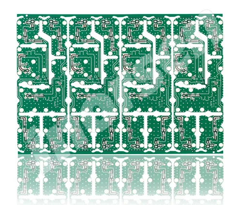
6-layer PCBs offer high-density solution for electronic systems requiring multiple signal and power planes. Ideal for high-speed digital circuits, the additional layers provide better signal integrity, reduced crosstalk, and improved EMI performance for demanding applications.
Quick Specifications
Technical Specifications
9 Parameters| Parameter | Specification |
|---|---|
|
Layer Count
Technical requirement
|
6
|
|
Layer Stackup
Technical requirement
|
Signal-Gnd-Signal-Signal-Pwr-Signal
|
|
Material Type
Technical requirement
|
FR-4 High Tg, Rogers Materials
|
|
Board Thickness
Technical requirement
|
1.0mm - 2.4mm
|
|
Copper Weight
Technical requirement
|
1-2oz (35-70μm)
|
|
Min Line/Space
Technical requirement
|
3.5mil/3.5mil
|
|
Min Hole Size
Technical requirement
|
0.15mm
|
|
Impedance Control
Technical requirement
|
±8%
|
|
Differential Pairs
Technical requirement
|
Yes
|
Manufacturing Process
7 StepsInner Layer Imaging
Step 1Photolithography for 4 inner layers
Layer Registration
Step 2Precision alignment of all layers
Lamination
Step 36-layer lamination process
Via Formation
Step 4Through-hole and microvias
Copper Plating
Step 5Uniform plating of all vias
Surface Finish
Step 6ENIG, ENEPIG, OSP
Final Testing
Step 7Impedance and electrical testing
Typical Applications
6 IndustriesReady to Get Started?
Contact our engineering team for a custom quote or explore our full range of PCB products.
Trusted by Global Clients
Real feedback from verified customers across the world