Product Features
High Precision Manufacturing
Advanced equipment ensures precise production
Strict Quality Control
100% electrical testing and visual inspection
Fast Turnaround
Quick delivery times for prototypes and mass production
Competitive Pricing
Cost-effective solutions without compromising quality
Quality Assurance
ISO Certified
ISO 9001:2015 & IATF 16949
UL Listed
UL 796 & UL 94V-0 Certified
100% Tested
Flying probe and AOI testing
12 Month Warranty
Comprehensive warranty coverage
Heavy Copper PCBs
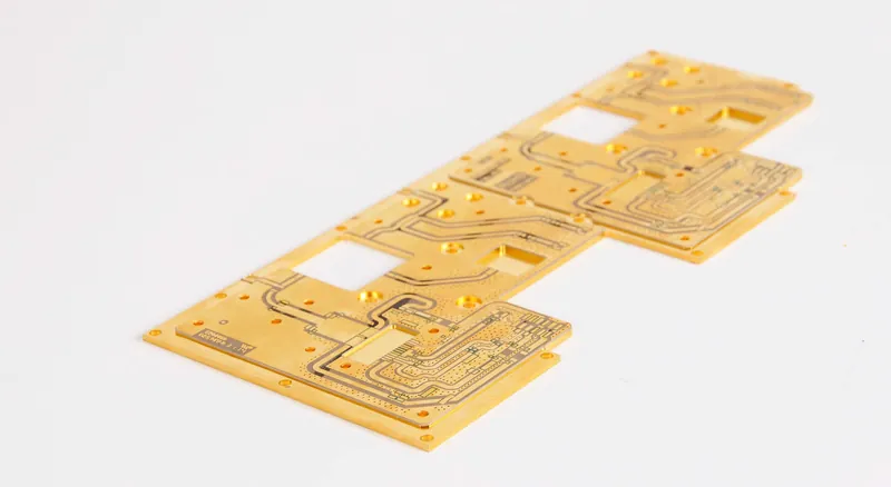
Heavy Copper PCBs feature copper thickness exceeding 3oz (105μm), enabling high current carrying capacity and thermal management. These boards are ideal for power electronics, automotive systems, and industrial applications requiring reliable high-current operation.
Quick Specifications
Technical Specifications
9 Parameters| Parameter | Specification |
|---|---|
|
Copper Weight
Technical requirement
|
3-20oz (105-700μm)
|
|
Layer Count
Technical requirement
|
1-20 Layers
|
|
Material Type
Technical requirement
|
FR-4 High Tg, Metal Core
|
|
Board Thickness
Technical requirement
|
1.0mm - 6.0mm
|
|
Min Line/Space
Technical requirement
|
6mil/6mil
|
|
Current Capacity
Technical requirement
|
Up to 400A
|
|
Thermal Conductivity
Technical requirement
|
1-4 W/mK
|
|
Surface Finish
Technical requirement
|
HASL, ENIG
|
|
Copper Plating
Technical requirement
|
Electroplated Heavy Copper
|
Manufacturing Process
7 StepsBase Material Prep
Step 1Thick substrate preparation
Copper Deposition
Step 2Electroplating to target thickness
Patterning
Step 3Thick copper photoimaging
Etching
Step 4Extended etch time process
Drilling
Step 5Large hole drilling
Surface Finish
Step 6
Testing
Step 7Current load testing
Typical Applications
6 IndustriesReady to Get Started?
Contact our engineering team for a custom quote or explore our full range of PCB products.
Trusted by Global Clients
Real feedback from verified customers across the world